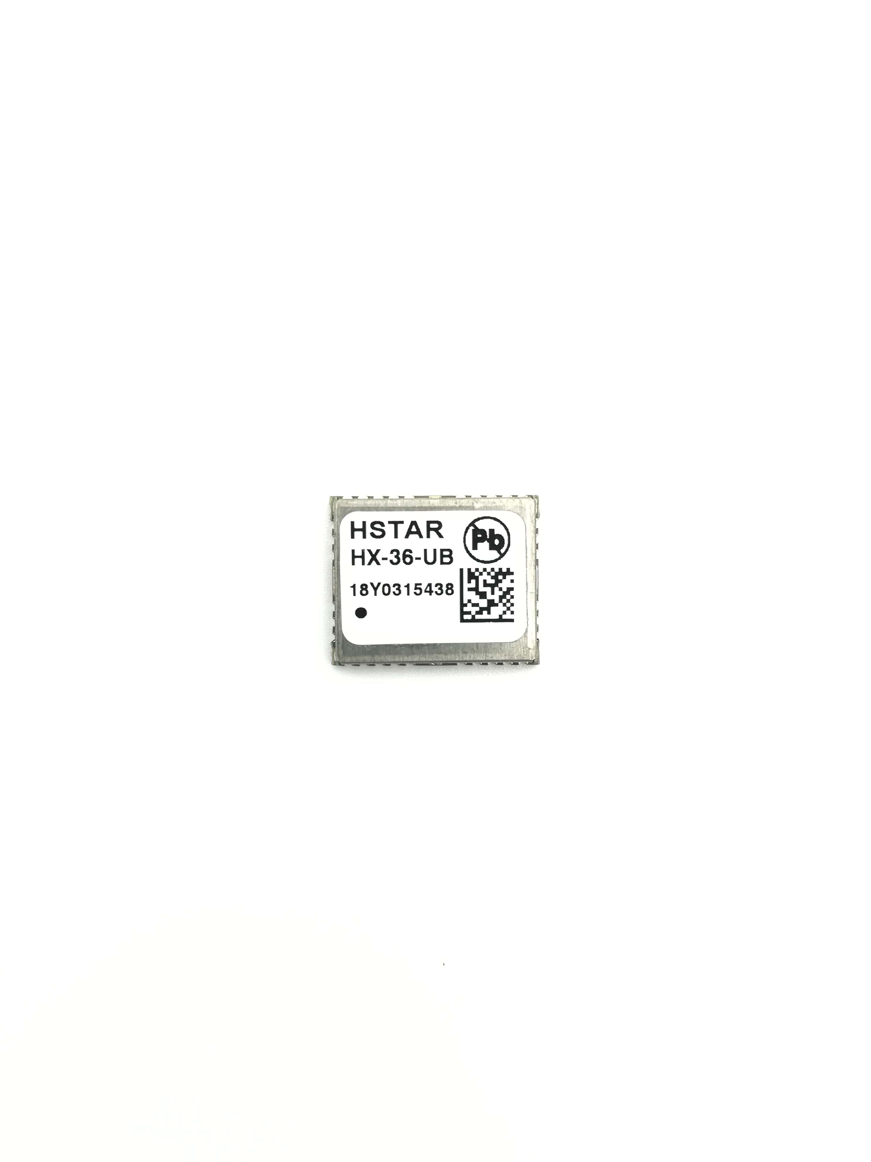
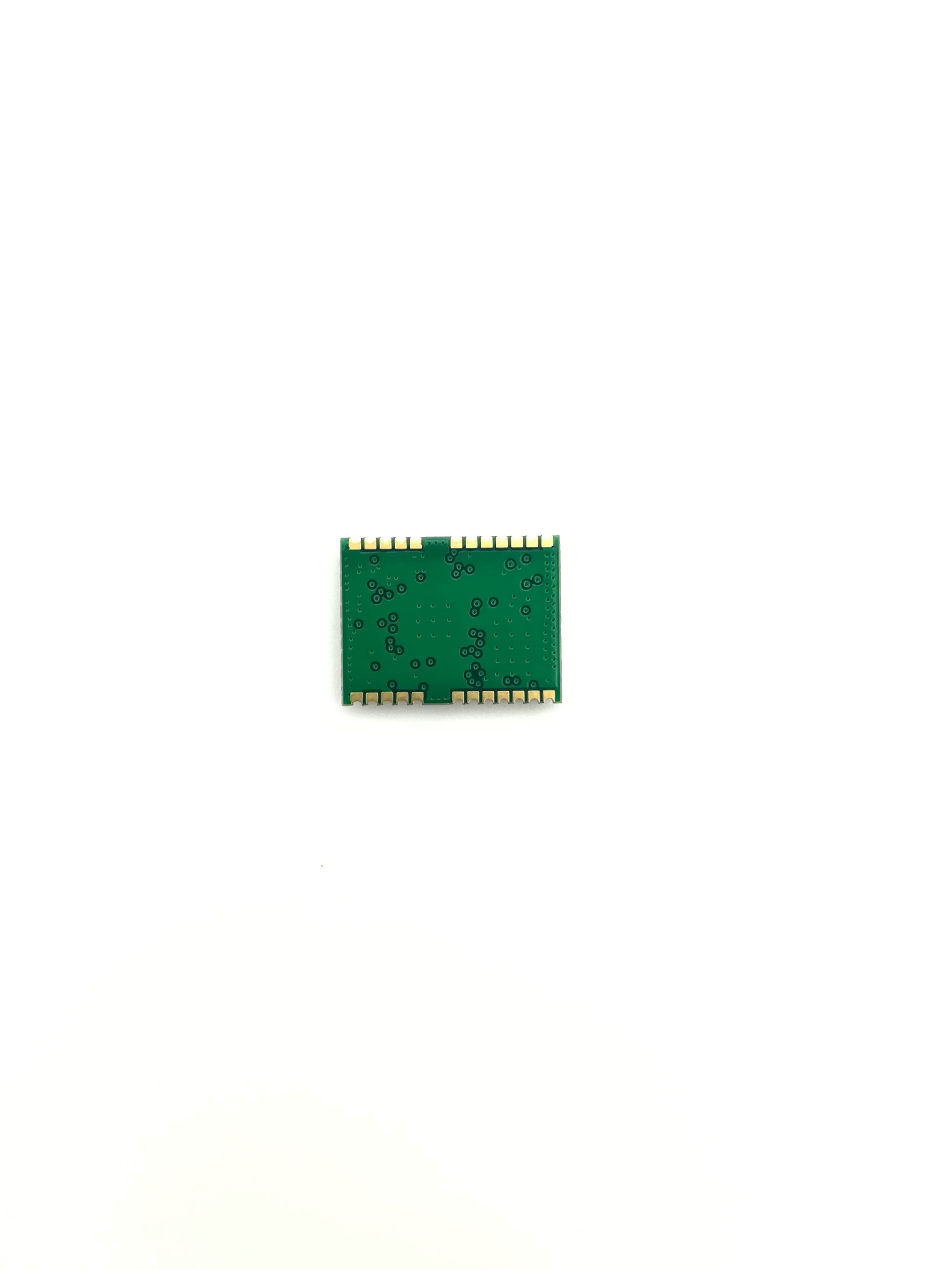
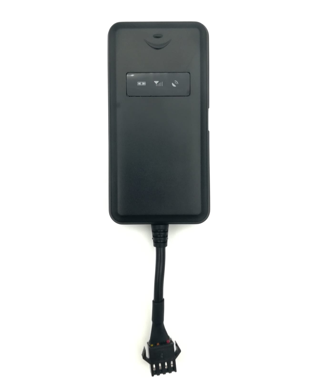
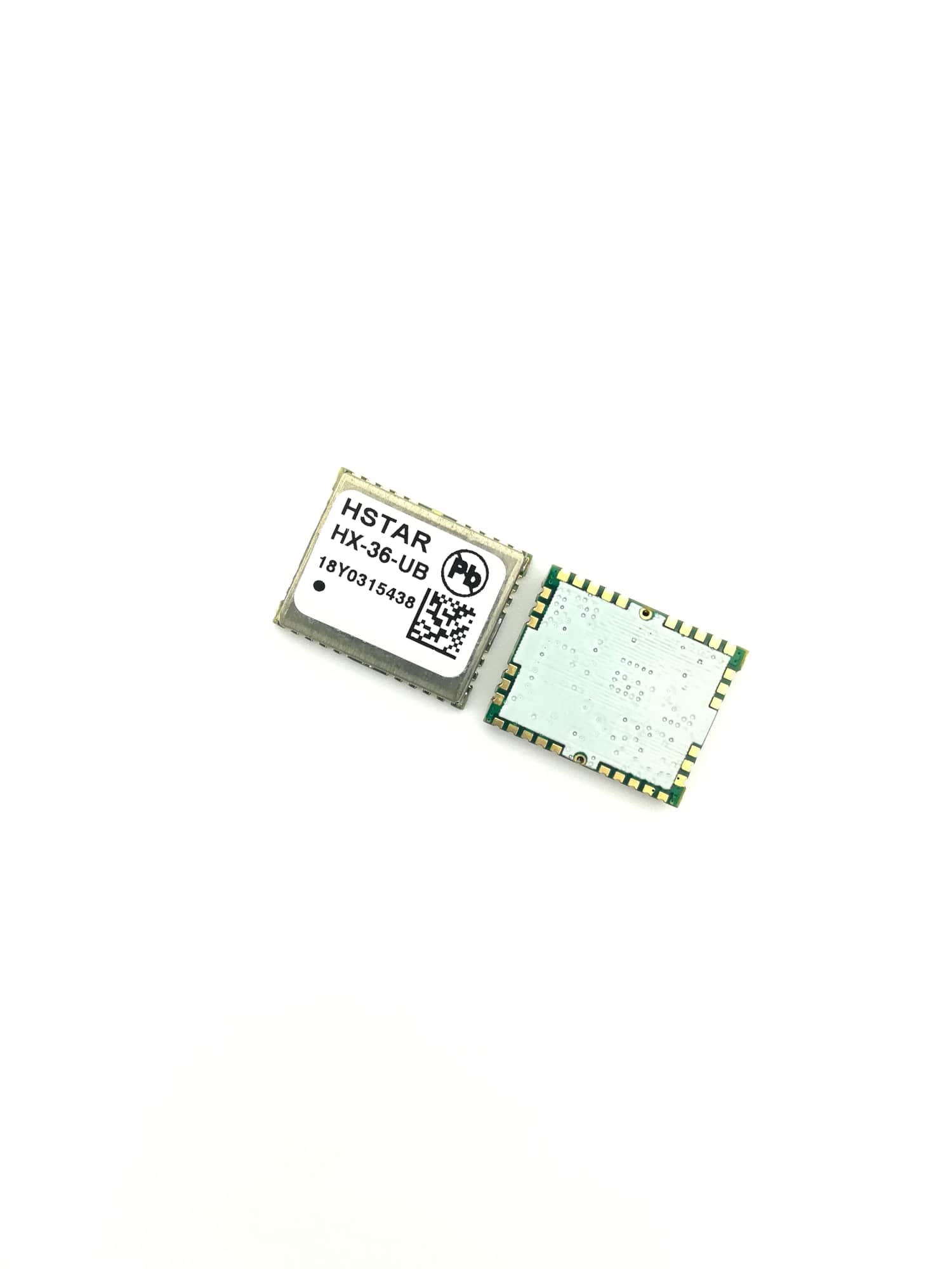
车载GPS模块
Pin No Module Name I/O Description 1 All GND Ground 2 All TXD O UART, leave open if not used, Voltage level referred VCC_IO. Can be configure
Pin No Module Name I/O Description 1 All GND Ground 2 All TXD O UART, leave open if not used, Voltage level referred VCC_IO. Can be configured as Data ready12 indication for the DDC interface. 3 All RXD I UART, leave open if not used, Volta......
咨询热线:13923438341
- 产品介绍
| Pin No | Module | Name | I/O | Description |
| 1 | All | GND | Ground | |
| 2 | All | TXD | O | UART, leave open if not used, Voltage level referred VCC_IO. Can be configured as Data ready12 indication for the DDC interface. |
| 3 | All | RXD | I | UART, leave open if not used, Voltage level referred VCC_IO |
| 4 | All | TIMEPULES | O | Pulse output at 1pulse per second aligned to the GPS signal. Leave open if not used, Voltage level referred VCC_IO |
| 5 | All | EXTINT | I | Can be used as an external wakeup signal. Leave open if not used, Voltage level referred VCC_IO |
| 6 | All | V-BCKP | I | Backup voltage input pin. Connect to GND if not used. |
| 7 | All | VCC_IO | IO supply voltage Input must be always supplied. Usually connect to VCC Pin 8 | |
| 8 | All | VCC |
Power supply of module(1.8-3.6V) |
|
| 9 | All | RSET-N | I | Must be connected to VCC always. Can be used as reset input pin with additional circuit (connected to VCC by 3k3 resistor) |
| 10 | All | GND | I | Ground |
| 11 | All | RF_IN | I |
Matched RF-Input, DC block inside. |
| 12 | All | GND | I | Ground |
| 13 | All | ANT_ON | O |
Active antenna or ext. LNA control pin in power save mode |
| 14 | All | VCC_RF | O | Can be used for active antenna or external LNA supply. |
| 15 | All | NC | Leave open. | |
| 16 | All | SDA | I/O | DDC Communication interface. Leave open if not used. |
| 17 | All | SCL | I/O | DDC Communication interface. Leave open if not used. |
| 18 | All | NC | Leave open. | |
|
Reserved Pin |


